| CPC G02B 6/12004 (2013.01) [H01L 24/19 (2013.01); H01L 24/20 (2013.01); H01L 25/167 (2013.01); H01L 25/18 (2013.01); H01L 31/02002 (2013.01); H01L 31/02327 (2013.01); H01L 24/08 (2013.01); H01L 24/32 (2013.01); H01L 24/80 (2013.01); H01L 2224/08145 (2013.01); H01L 2224/211 (2013.01); H01L 2224/32145 (2013.01); H01L 2224/80895 (2013.01); H01L 2224/80896 (2013.01)] | 20 Claims |
|
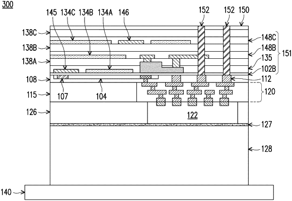
1. A method, comprising:
patterning a silicon layer to form a first waveguide, wherein the silicon layer is on a first side of a buried oxide layer, wherein the buried oxide layer is over a substrate;
forming a first redistribution structure over the first waveguide;
bonding a first semiconductor die to the first redistribution structure;
removing the substrate to expose a second side of the buried oxide layer, wherein the second side of the buried oxide layer is opposite the first side of the buried oxide layer;
forming a second waveguide on the second side of the buried oxide layer;
forming a first dielectric layer over the second waveguide and over the second side of the buried oxide layer; and
forming a through via extending through the first dielectric layer to electrically and physically contact the first redistribution structure.
|