| CPC G02B 3/0062 (2013.01) [B29C 39/026 (2013.01); G02B 27/4272 (2013.01)] | 11 Claims |
|
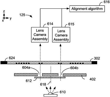
1. A method of aligning a stencil to an eyepiece wafer, the method comprising:
providing the stencil;
positioning the stencil with respect to a first light source;
determining locations of at least two stencil apertures;
providing the eyepiece wafer, wherein the eyepiece wafer includes at least two eyepiece waveguides, each eyepiece waveguide including an incoupling grating and a corresponding diffraction pattern;
directing light from one or more second light sources to impinge on each of the corresponding diffraction patterns and propagate through each corresponding eyepiece waveguide by total internal reflection;
imaging light diffracted from each incoupling grating;
determining at least two incoupling grating locations;
determining offsets between corresponding stencil aperture locations and incoupling grating locations; and
aligning the stencil to the eyepiece wafer based on the determined offsets.
|