| CPC H10N 52/101 (2023.02) [G01R 33/077 (2013.01); H10N 52/01 (2023.02); H10N 52/80 (2023.02)] | 19 Claims |

|
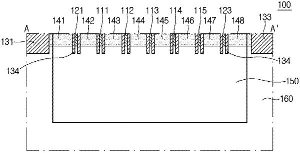
1. A semiconductor device, comprising:
a N-type sensing region disposed on a semiconductor substrate;
P-type contact regions and N-type contact regions which are disposed alternately in the N-type sensing region;
at least one first trench, disposed adjacent to at least one of the P-type contact regions, and configured to have a first width; and
a plurality of second trenches, which are configured to separate each of the P-type contact regions and each of the N-type contact regions, and are configured to have a second width less than the first width of the at least one first trench,
wherein a width of each of the N-type contact regions is less than a width of each of the P-type contact regions, and
wherein each of the P-type contact regions is configured to have a same width as each other.
|