| CPC H10N 50/01 (2023.02) [H10N 50/10 (2023.02)] | 10 Claims |

|
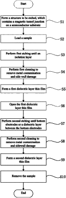
1. A method for etching a magnetic tunnel junction, using an etching device comprising a sample loading chamber, a vacuum transition chamber, a reactive ion plasma etching chamber, an ion beam etching chamber, a film coating chamber, and a vacuum transport chamber, the vacuum transition chamber being communicatively connected to the sample loading chamber and the vacuum transport chamber separately, the reactive ion plasma etching chamber, the ion beam etching chamber, and the film coating chamber being communicatively connected separately to the vacuum transport chamber, wherein without interrupting a vacuum, a wafer is processed and treated in the reactive ion plasma etching chamber, the ion beam etching chamber, and the film coating chamber according to the following steps, and the ion beam etching chamber and the reactive ion plasma etching chamber are separately used at least once,
the method comprising the following steps:
a sample preparation step: forming a structure to be etched, which contains a bottom electrode metal layer, a magnetic tunnel junction, a cap layer, and a mask layer on a semiconductor substrate, wherein the magnetic tunnel junction comprises a fixed layer, an isolation layer, and a free layer;
a sample loading step: loading a sample to the sample loading chamber, and the sample entering the vacuum transport chamber through the vacuum transition chamber;
a first etching step: the sample entering the reactive ion plasma etching chamber or the ion beam etching chamber, etching the sample and stopping etching when the isolation layer is reached; and then the sample returning to the vacuum transport chamber;
a first cleaning step: the sample entering the reactive ion plasma etching chamber or the ion beam etching chamber, and removing metallic residues and treating a sample surface, so that metal contamination and a sidewall damage layer formed in the first etching step are completely removed; and then the sample returning to the vacuum transport chamber;
a first dielectric coating step: the sample entering the film coating chamber, and forming a first dielectric thin film on the upper surface of and around the sample; and then the sample returning to the vacuum transport chamber;
a first dielectric thin film opening step: the sample entering the reactive ion plasma etching chamber or the ion beam etching chamber, opening the first dielectric thin film on the top and bottom portions of the device but leaving the part on a device sidewall, and stopping etching; and then the sample returning to the vacuum transport chamber;
a second etching step: the sample entering the reactive ion plasma etching chamber or the ion beam etching chamber, etching the sample, and stopping etching when the bottom electrode metal layer or a dielectric layer between the bottom electrode metal layers is reached; and then the sample returning to the vacuum transport chamber;
a second cleaning step: the sample entering the reactive ion plasma etching chamber or the ion beam etching chamber, and removing metallic residues and treating a sample surface, so that metal contamination and a sidewall damage layer formed in the second etching step are completely removed and part or all of the first dielectric thin film layer is removed; and then the sample returning to the vacuum transport chamber;
a second dielectric coating step: the sample entering the film coating chamber for coating protection, and forming a second dielectric thin film on the upper surface of and around the sample; and then, the sample returning to the vacuum transport chamber; and
a sample removal step: the sample returning from the vacuum transport chamber to the sample loading chamber through the vacuum transition chamber,
wherein a material of the first dielectric thin film or the second dielectric thin film is a group IV oxide, group IV nitride, group IV nitrogen oxide, transition metal oxide, transition metal nitride, transition metal nitrogen oxide, alkaline earth metal oxide, alkaline earth metal nitride, alkaline earth metal nitrogen oxide, or a combination thereof.
|