US 12,035,624 B2
OFETs having multilayer organic semiconductor with high on/off ratio
Tingling Rao, Bellevue, WA (US); Lafe Joseph Purvis, II, Redmond, WA (US); Tanya Malhotra, Houston, TX (US); and Andrew John Ouderkirk, Kirkland, WA (US)
Assigned to Meta Platforms Technologies, LLC, Menlo Park, CA (US)
Filed by Meta Platforms Technologies, LLC, Menlo Park, CA (US)
Filed on Mar. 7, 2023, as Appl. No. 18/179,925.
Application 18/179,925 is a continuation of application No. 17/098,493, filed on Nov. 16, 2020, granted, now 11,631,818.
Claims priority of provisional application 63/061,971, filed on Aug. 6, 2020.
Prior Publication US 2023/0210003 A1, Jun. 29, 2023
Int. Cl. H01L 23/00 (2006.01); H10K 10/46 (2023.01); H10K 71/10 (2023.01); H10K 85/10 (2023.01); H10K 85/40 (2023.01); H10K 85/60 (2023.01)
CPC H10K 85/6572 (2023.02) [H10K 10/486 (2023.02); H10K 71/191 (2023.02); H10K 85/10 (2023.02); H10K 85/40 (2023.02); H10K 85/6574 (2023.02); H10K 85/6576 (2023.02)] 12 Claims
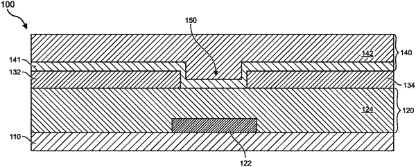
OG exemplary drawing
 
1. A method comprising:
forming a first photoalignment layer;
illuminating the first photoalignment layer with polarized light to form a first oriented photoalignment layer;
forming a first organic semiconductor layer directly over the first oriented photoalignment layer;
forming a second photoalignment layer over the first organic semiconductor layer;
illuminating the second photoalignment layer with polarized light to form a second oriented photoalignment layer; and
forming a second organic semiconductor layer directly over the second oriented photoalignment layer.