| CPC H10K 77/111 (2023.02) [H10K 59/126 (2023.02); H10K 71/00 (2023.02); H10K 71/80 (2023.02); H10K 59/1201 (2023.02); H10K 2102/00 (2023.02); H10K 2102/311 (2023.02); H10K 2102/351 (2023.02)] | 18 Claims |

|
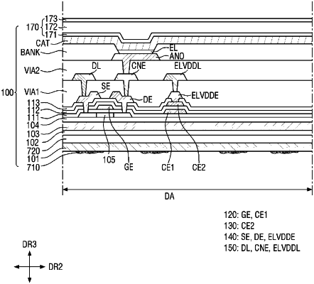
1. A display device comprising:
a first flexible substrate;
a first barrier layer disposed on a surface of the first flexible substrate;
a thin film transistor layer disposed on a surface of the first barrier layer; and
an inorganic layer disposed on an opposing surface of the first flexible substrate;
wherein the inorganic layer is disposed to cover a first portion of the opposing surface of the first flexible substrate and to expose a second portion of the opposing surface of the first flexible substrate,
wherein the inorganic layer comprises a plurality of sub-inorganic layers,
the plurality of sub-inorganic layers are separated from each other,
each of the plurality of sub-inorganic layers contacts the first portion of the opposing surface of the first flexible substrate, and
a space between adjacent sub-inorganic layers overlaps the second portion of the opposing surface of the first flexible substrate.
|