| CPC H10K 59/88 (2023.02) [H10K 50/844 (2023.02); H10K 59/122 (2023.02); H10K 77/10 (2023.02)] | 9 Claims |
|
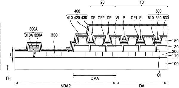
1. A display device, comprising:
a substrate;
a non-display portion defined in the substrate
a first insulating layer disposed on the substrate;
a second insulating layer disposed on the first insulating layer;
a plurality of pixels surrounding at least a portion of the non-display portion,
wherein each pixel comprises a light-emitting element comprising a pixel electrode, and a plurality of openings disposed on the second insulating layer and exposing the pixel electrode and a first pixel circuit disposed on the substrate; and
a plurality of dummy pixels disposed between the non-display portion and the pixels, wherein each dummy pixel comprises a second pixel circuit disposed on the substrate
wherein the second insulating layer corresponding to one of the plurality of dummy pixels is flat.
|