| CPC H10K 59/40 (2023.02) [G06F 3/0446 (2019.05); H10K 50/844 (2023.02); H10K 50/865 (2023.02); H10K 59/122 (2023.02)] | 13 Claims |

|
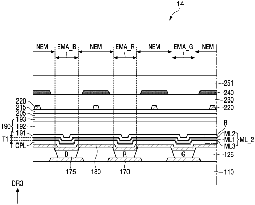
1. A display device comprising:
a substrate;
a first electrode on the substrate;
a bank layer partially exposing a top surface of the first electrode;
a light emitting layer disposed on the partially exposed top surface of the first electrode;
a second electrode on the light emitting layer and the bank layer;
an inorganic deposition layer on the second electrode;
a thin film encapsulation layer on the inorganic deposition layer; and
a capping layer disposed between the inorganic deposition layer and the second electrode,
wherein the inorganic deposition layer comprises:
a first inorganic deposition layer;
a second inorganic deposition layer directly disposed between the first inorganic deposition layer and the thin film encapsulation layer; and
a third inorganic deposition layer directly disposed between the first inorganic deposition layer and the capping layer,
wherein the first inorganic deposition layer contains ytterbium (Yb), and each of the second inorganic deposition layer and the third inorganic deposition layer contains bismuth (Bi),
wherein a thickness of the first inorganic deposition layer is greater than a thickness of each of the second inorganic deposition layer and the third inorganic deposition layer.
|