| CPC H10K 59/131 (2023.02) [G09G 3/3225 (2013.01); G09G 3/3266 (2013.01); H10K 50/11 (2023.02); H10K 59/1213 (2023.02); H10K 59/1216 (2023.02); H10K 59/122 (2023.02); H10K 59/352 (2023.02); H10K 71/00 (2023.02); G09G 2300/0426 (2013.01); H01L 27/124 (2013.01); H01L 27/1255 (2013.01); H10K 59/1201 (2023.02)] | 18 Claims |

|
1. A display substrate comprising:
a base substrate;
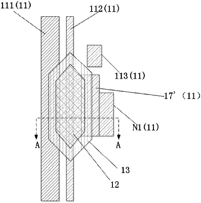
a first conductive layer on the base substrate, the first conductive layer comprising a first signal line, a second signal line, and an additional pad layer which are spaced apart from each other; and
a first electrode on a side of the first conductive layer away from the base substrate,
wherein the first electrode comprises a first side portion and a second side portion opposite to each other, an orthographic projection of the first side portion on the base substrate and an orthographic projection of the first signal line on the base substrate have a first overlapping region, an orthographic projection of the second end portion on the base substrate and an orthographic projection of the additional pad layer on the base substrate have a second overlapping region, and the orthographic projection of the first side portion on the base substrate and the orthographic projection of the second side portion on the base substrate are respectively located on both sides of an orthographic projection of the second signal line on the base substrate, and
wherein the first conductive layer further comprises a first electrical connection portion, an orthographic projection of the first electrical connection portion on the base substrate does not overlap an orthographic projection of the second overlapping region on the base substrate.
|