| CPC H10K 59/131 (2023.02) [H10K 59/1213 (2023.02); H10K 59/1216 (2023.02)] | 17 Claims |

|
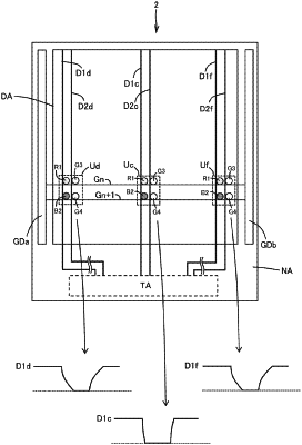
1. A display device having a display area, a frame area, and a terminal area along an edge of the frame area, the display device comprising:
a plurality of data signal lines extending in a column direction;
a plurality of scan signal lines extending in a row direction so as to intersect with the plurality of data signal lines;
a scan control circuit in the frame area along at least one of column-wise extending edges of the display area, the scan control circuit being configured to feed a scan signal to the plurality of scan signal lines; and
a plurality of pixel circuits each associated with a different one of intersections of the plurality of data signal lines and the plurality of scan signal lines, each of the plurality of pixel circuits including: a light-emitting element; a drive transistor configured to control a current in the light-emitting element; and a capacitive element connected to a control terminal of the drive transistor to retain a data voltage, wherein
the plurality of pixel circuits includes a plurality of groups each including: a first pixel circuit configured to emit light of a first color; a second pixel circuit located adjacent to the first pixel circuit and configured to emit light of a second color that differs from the first color; a third pixel circuit located adjacent to the first pixel circuit and configured to emit light of a third color that differs from the first color and the second color; and a fourth pixel circuit located adjacent to the third pixel circuit and configured to emit light of the third color,
in each of the plurality of groups, the first pixel circuit and the second pixel circuit are connected to a first data signal line, the third pixel circuit and the fourth pixel circuit are connected to a second data signal line, the first pixel circuit and the third pixel circuit are connected to a first scan signal line, and the second pixel circuit and the fourth pixel circuit are connected to a second scan signal line, and
of those two of the first pixel circuits which are included in different ones of the plurality of groups and connected to a common one of the first scan signal lines, the capacitive element in the first pixel circuit that is located farther in the row direction from a center of the display area has a larger capacitance value than does the capacitive element in the first pixel circuit that is located closer in the row direction to the center of the display area.
|