| CPC H10K 59/131 (2023.02) | 20 Claims |

|
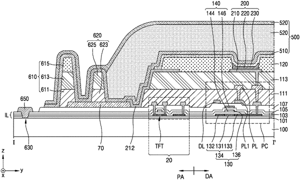
1. A display device comprising:
a substrate including a display area and a peripheral area around the display area;
a thin-film transistor disposed on the substrate in the display area and a display element electrically connected to the thin-film transistor; and
a first voltage line and a second voltage line located on the substrate in the peripheral area and supplying power to drive the display element,
wherein the first voltage line is a common voltage line and entirely surrounds the display area,
the second voltage line is a driving voltage line and is disposed to correspond to one side of the display area, and
the first voltage line and the second voltage line are disposed on different layers, and
wherein the first voltage line at least partially overlaps with at least one partition disposed in the peripheral area.
|