| CPC H10K 59/131 (2023.02) [H10K 50/115 (2023.02); H10K 50/813 (2023.02); H10K 50/822 (2023.02); H10K 59/123 (2023.02); H10K 59/124 (2023.02); H10K 59/352 (2023.02); H10K 59/353 (2023.02); H10K 71/00 (2023.02); H10K 2102/351 (2023.02)] | 18 Claims |

|
1. A display device comprising:
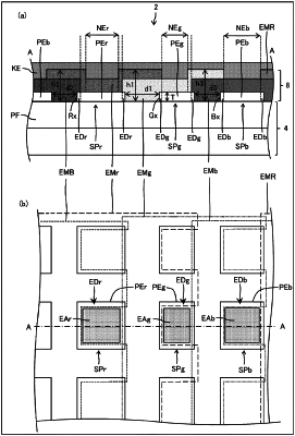
an organic insulating film formed to cover a first thin film transistor (TFT) and including a first contact hole, the first contact hole being provided with a first inclined face;
a first pixel electrode formed on the first contact hole and the organic insulating film;
a first intra-pixel wiring line formed under the organic insulating film and electrically connected to the first pixel electrode via the first contact hole, the first intra-pixel wiring line being electrically connected to the first TFT;
a first light-emitting layer formed on the organic insulating film, and covering the first pixel electrode;
a second light-emitting layer corresponding to a second pixel electrode adjacent to the first pixel electrode, the second light-emitting layer being formed to overlap the first light-emitting layer at least in the first inclined face of the first contact hole; and
a common electrode formed on the first light-emitting layer to cover the first pixel electrode, wherein
the first light-emitting layer and the second light-emitting layer include quantum dots,
the first light-emitting layer overlaps the second light-emitting layer at a peripheral edge portion of the first pixel electrode, and
the first light-emitting layer and the second light-emitting layer cover the peripheral edge portion of the first pixel electrode.
|