| CPC H10K 59/131 (2023.02) | 20 Claims |

|
1. A display device comprising:
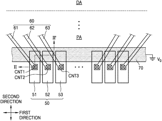
a substrate comprising a display area at which an image is displayed by a pixel, and a peripheral area around the display area;
a pad portion at the peripheral area, and comprising a first pad and a second pad adjacent to each other;
a fan-out wire portion comprising a first fan-out wire below the first pad and connected to the first pad through a first contact hole to extend to the display area, and a second fan-out wire below the second pad and connected to the second pad through a second contact hole to extend to the display area; and
a conductive layer between an upper portion of the fan-out wire portion and a lower portion of the pad portion, and at least partially corresponding to an overlapping area of the fan-out wire portion and the pad portion,
wherein the second fan-out wire at least partially overlaps with the first pad in a plan view.
|