| CPC H10K 59/131 (2023.02) | 18 Claims |

|
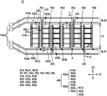
1. A display device comprising:
a first pixel stem wiring and a common stem wiring extending in a first direction and spaced apart from each other;
a first pixel branch wiring branched from the first pixel stem wiring and extending in a second direction crossing the first direction, the first pixel branch wiring comprising a base branch pattern connected to the first pixel stem wiring, a separate branch pattern spaced apart from the base branch pattern, and a bridge wiring connecting the base branch pattern to the separate branch pattern;
a common branch wiring branched from the common stem wiring and extending in the second direction;
a first light emitting element between the first pixel branch wiring and the common branch wiring;
a second pixel stem wiring extending in the first direction and spaced apart from the first pixel stem wiring and the common stem wiring;
a second pixel branch wiring branched from the second pixel stem wiring and extending in the second direction; and
a second light emitting element between the second pixel branch wiring and the common branch wiring,
wherein the first pixel stem wiring, the base branch pattern, and the separate branch pattern are in a first conductive layer,
wherein the bridge wiring is in a second conductive layer on a different layer than the first conductive layer, and
wherein the first light emitting elements are between the common branch wiring and the separate branch pattern.
|