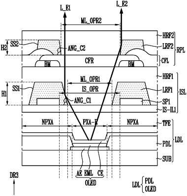
| CPC H10K 50/858 (2023.02) [G06F 3/0443 (2019.05); H10K 50/86 (2023.02); H10K 50/865 (2023.02); H10K 59/122 (2023.02); H10K 59/38 (2023.02); H10K 59/40 (2023.02); H10K 2102/351 (2023.02)] | 19 Claims |

|
1. A display device comprising:
a pixel defining layer on a substrate and defining a light emission area;
a light emitting element layer in the light emission area;
a sensing electrode on the pixel defining layer;
a first organic layer covering the sensing electrode and having sidewalls defining an opening therebetween corresponding to the light emission area;
an anti-reflection layer on the first organic layer; and
a second organic layer between the first organic layer and the anti-reflection layer and filled in the opening of the first organic layer, the second organic layer contacting the sidewalls of the first organic layer.
|