| CPC H10K 50/856 (2023.02) [G03G 15/04036 (2013.01); H04N 23/53 (2023.01); H10K 59/123 (2023.02); H10K 71/00 (2023.02); H10K 59/1201 (2023.02); H10K 59/38 (2023.02)] | 20 Claims |
|
1. A light emitting device in which a plurality of light emitting elements are arranged on a main surface of a substrate,
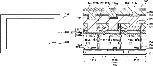
wherein each of the plurality of light emitting elements comprises a light emitting layer, a reflective layer arranged between the light emitting layer and the main surface of the substrate and configured to reflect light generated by the light emitting layer, a first electrode arranged between the reflective layer and the light emitting layer, an optical distance adjustment layer arranged between the reflective layer and the first electrode, an insulating layer covering a peripheral edge portion of the first electrode and arranged, between two light emitting elements adjacent to each other in the plurality of light emitting elements, between the optical distance adjustment layer and the light emitting layer, and a conductive plug extending from the insulating layer to pass through the optical distance adjustment layer and reach a height of an upper surface of the reflective layer while being in electrical contact with the first electrode.
|