| CPC H10K 50/85 (2023.02) [H10K 59/12 (2023.02); H10K 59/38 (2023.02)] | 19 Claims |

|
1. A display device, comprising:
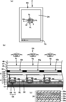
a light-emitting element layer including a plurality of light-emitting elements, the plurality of light-emitting elements including a thin film transistor (TFT) layer, a plurality of first electrodes, a light-emitting layer, and a second electrode,
wherein, on a light emission side of the light-emitting element layer, each of a plurality of wavelength conversion layers corresponding to each of the plurality of light-emitting elements, a dielectric layer, and a particle layer are provided in this order,
the particle layer includes metal nanoparticles including a core and a shell around the core, and
the dielectric layer and the particle layer are commonly provided above the plurality of light emitting elements.
|