| CPC H10K 50/844 (2023.02) [H10K 59/12 (2023.02); H10K 77/10 (2023.02)] | 19 Claims |
|
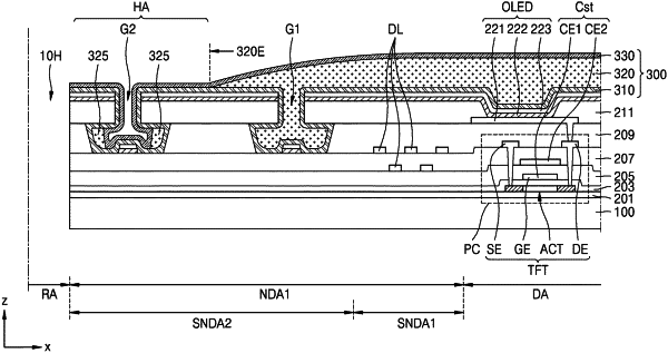
1. A display panel, comprising:
a substrate having an opening;
a plurality of light-emitting diodes on the substrate, the plurality of light-emitting diodes arranged in a display area surrounding the opening, the plurality of light-emitting diodes comprising a first light-emitting diode including a first electrode, a second electrode, and an intermediate layer between the first electrode and the second electrode;
a multilayer film comprising:
a first layer; and
a second layer on the first layer,
wherein the multilayer film comprises a first groove between the opening of the substrate and the display area, a part of the second layer includes a tip extending in a width direction such that the first groove has an undercut structure,
an inorganic insulating layer under the first groove of the multilayer film; and
an encapsulation layer on the light-emitting diode and the first groove, the encapsulation layer comprising a first inorganic encapsulation layer, an organic encapsulation layer, and a second inorganic encapsulation layer.
|