US 12,035,549 B2
Solid state image sensor, production method thereof and electronic device
Masahiro Joei, Kanagawa (JP); and Kaori Takimoto, Kanagawa (JP)
Assigned to SONY SEMICONDUCTOR SOLUTIONS CORPORATION, Kanagawa (JP)
Filed by SONY SEMICONDUCTOR SOLUTIONS CORPORATION, Kanagawa (JP)
Filed on Oct. 7, 2022, as Appl. No. 17/962,244.
Application 17/962,244 is a continuation of application No. 17/068,398, filed on Oct. 12, 2020, granted, now 11,489,015.
Application 17/068,398 is a continuation of application No. 16/378,339, filed on Apr. 8, 2019, granted, now 10,840,303, issued on Nov. 17, 2020.
Application 16/378,339 is a continuation of application No. 16/018,879, filed on Jun. 26, 2018, granted, now 10,304,904, issued on May 28, 2019.
Application 16/018,879 is a continuation of application No. 15/589,681, filed on May 8, 2017, granted, now 10,014,349, issued on Jul. 3, 2018.
Application 15/589,681 is a continuation of application No. 14/477,639, filed on Sep. 4, 2014, granted, now 9,666,643, issued on May 30, 2017.
Claims priority of application No. 2013-189723 (JP), filed on Sep. 12, 2013.
Prior Publication US 2023/0034528 A1, Feb. 2, 2023
Int. Cl. H01L 27/30 (2006.01); H01L 27/146 (2006.01); H01L 51/44 (2006.01); H10K 30/81 (2023.01); H10K 39/32 (2023.01)
CPC H10K 39/32 (2023.02) [H01L 27/14643 (2013.01); H10K 30/81 (2023.02)] 20 Claims
OG exemplary drawing
 
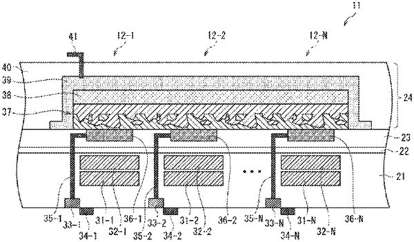
1. A solid state image sensor, comprising:
a semiconductor substrate where photoelectric conversion regions for converting light into charges are arranged per a plurality of pixels planarly arranged;
an organic photoelectric conversion film laminated at a light irradiated side of the semiconductor substrate via a first insulation film and formed at the regions where a plurality of the pixels are formed;
a lower electrode formed at and in contact with the organic photoelectric conversion film at a semiconductor substrate side;
a first upper electrode laminated at a light irradiated side of the organic photoelectric conversion film and formed such that ends of the first upper electrode substantially conform with ends of the organic photoelectric conversion film when the solid state image sensor is planarly viewed; and
a film stress suppressor for suppressing an effect of a film stress on the organic photoelectric conversion film, the film stress being generated on the first upper electrode and provided above the lower electrode at each instance.