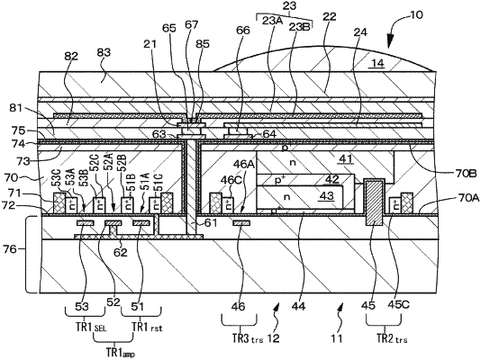
| CPC H10K 30/10 (2023.02) [H10K 39/32 (2023.02); H10K 85/211 (2023.02)] | 14 Claims |

|
1. An image pickup element, comprising:
a first electrode;
a charge accumulation electrode arranged apart from the first electrode;
a photoelectric conversion unit that contacts the first electrode and is formed above the charge accumulation electrode via an insulation layer; and
a second electrode formed on the photoelectric conversion unit, wherein
the photoelectric conversion unit includes, from a second-electrode side, a photoelectric conversion layer, and an inorganic oxide semiconductor material layer including a composite oxide of an indium oxide, a gallium oxide, and a tin oxide,
the composite oxide is InaGabSncOd,
a indicates an atomic ratio of indium (In) atoms,
b indicates an atomic ratio of gallium (Ga) atoms,
c indicates an atomic ratio of tin (Sn) atoms, and
0.30≤b/(a+b+c)≤0.50 and b≥c are satisfied.
|