| CPC H10K 59/122 (2023.02) [H10K 50/813 (2023.02); H10K 50/822 (2023.02); H10K 50/824 (2023.02); H10K 59/1315 (2023.02); H10K 71/00 (2023.02); H10K 50/15 (2023.02); H10K 50/17 (2023.02); H10K 59/1201 (2023.02)] | 10 Claims |

|
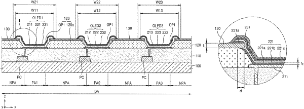
1. An organic light-emitting display apparatus comprising:
a substrate including a pixel area and a non-pixel area in a display area;
a pixel electrode corresponding to the pixel area;
a pixel-defining layer comprising a cover portion and an opening, wherein the cover portion covers an edge of the pixel electrode, and the opening exposes a central portion of the pixel electrode;
a conductive layer located to correspond to at least a portion of a top surface of the cover portion; and
an intermediate layer and a counter electrode located in the opening,
wherein at least a portion of the intermediate layer is in contact with the conductive layer, and the pixel-defining layer comprises an inorganic material, and
wherein a portion of a lower surface of the conductive layer contacts the top surface of the cover portion and another portion of the lower surface of conductive layer is spaced apart from the top surface of the cover portion.
|