| CPC H10B 63/845 (2023.02) [H10B 53/20 (2023.02); H10B 63/20 (2023.02); H10B 63/22 (2023.02); H10B 63/24 (2023.02); H10B 63/80 (2023.02); H10B 63/84 (2023.02); H10N 70/235 (2023.02); H10N 70/245 (2023.02)] | 19 Claims |
|
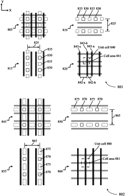
12. An apparatus, comprising:
a stack that includes an electrode layer and a memory layer;
a conductive element in contact with the stack;
a conductive plug that extends through the stack and is coupled with the conductive element, the conductive plug having a first width at the memory layer and a second width at the electrode layer, the second width larger than the first width;
a first electrode at the electrode layer, the first electrode coupled with the conductive plug; and
a conformal liner at a second electrode layer within the stack, the conformal liner interposed between the conductive plug and a dielectric material.
|