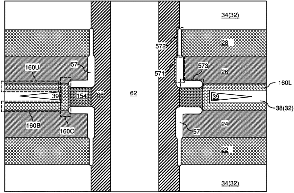
| CPC H10B 51/20 (2023.02) [H01L 29/7606 (2013.01); H10B 41/27 (2023.02); H10B 43/27 (2023.02); H01L 29/16 (2013.01); H01L 29/1606 (2013.01); H01L 29/161 (2013.01); H01L 29/2003 (2013.01); H01L 29/24 (2013.01)] | 6 Claims |

|
1. A three-dimensional memory device, comprising:
an alternating stack of source layers and drain layers located over a substrate;
a memory opening vertically extending through the alternating stack;
a vertical word line located in the memory opening and vertically extending through each of the source layers and the drain layers of the alternating stack;
discrete semiconductor channels contacting horizontal surfaces of a respective vertically neighboring pair of a source layer of the source layers and a drain layer of the drain layers; and
a vertical stack of discrete memory material portions laterally surrounding the vertical word line;
wherein each of the discrete semiconductor channels comprises a semiconductor channel layer including a cylindrical channel portion, an upper horizontally-extending portion adjoined to a top end of the cylindrical channel portion, and a lower horizontally-extending portion adjoined to a bottom end of the cylindrical channel portion.
|