| CPC H10B 43/27 (2023.02) [H01L 21/3213 (2013.01); H01L 21/76802 (2013.01); H01L 21/76877 (2013.01); H01L 29/41775 (2013.01); H01L 29/66666 (2013.01); H01L 29/7827 (2013.01); H01L 29/7889 (2013.01); H01L 29/7926 (2013.01); H10B 41/27 (2023.02); H10B 41/40 (2023.02); H10B 43/10 (2023.02); H10B 43/35 (2023.02); H10B 43/40 (2023.02); H10B 43/50 (2023.02)] | 19 Claims |
|
1. A semiconductor device, comprising:
a substrate having a first region and a second region;
gate electrodes stacked perpendicularly on an upper surface of the substrate in the first region, the gate electrodes extending to different lengths in a first direction in the second region, and each of the gate electrodes including:
subgate electrodes spaced apart from each other in a second direction perpendicular to the first direction, and
a gate connection portion connecting to each other subgate electrodes at a same level;
channels extending through the gate electrodes perpendicularly to the upper surface of the substrate in the first region; and
dummy channels extending through the gate electrodes perpendicularly to the upper surface of the substrate, the dummy channels including:
first dummy channels arranged in the second region in rows and columns, the rows extending in the first direction, and the columns extending in the second direction, and
a second dummy channel passing through the gate connection portion in the second region, the second dummy channel being arranged between two columns of the first dummy channels that are adjacent to each other along the first direction,
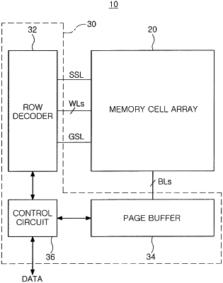
wherein the first region is a memory cell region including a plurality of memory cells along the channels, and the second region electrically connects the memory cell region and a control logic region driving the plurality of memory cells.
|