| CPC H10B 43/27 (2023.02) [H01L 23/5283 (2013.01); H10B 41/10 (2023.02); H10B 41/27 (2023.02); H10B 43/10 (2023.02)] | 20 Claims |

|
1. A method for fabricating a semiconductor device, comprising:
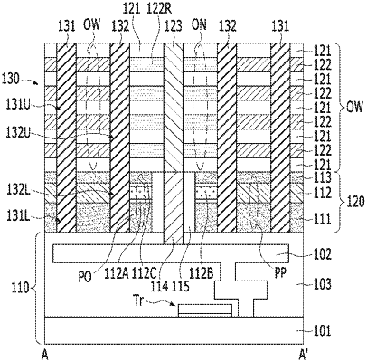
forming a source structure over a lower structure with interconnections;
forming a first contact plug that penetrates the source structure to be coupled to the interconnections, and a sacrificial pad that penetrates the source structure and is spaced apart from the first contact plug;
forming an upper structure that covers the sacrificial pad, the first contact plug, and the source structure, the upper structure including a first region and a second region, and each of the first and second regions including first alternating stack of dielectric layers and sacrificial layers;
forming a second contact plug that penetrates the first region of the upper structure and contacts the first contact plug;
forming a dummy sacrificial pad that penetrates the first region of the upper structure to contact the sacrificial pad and is spaced apart from the second contact plug, the dummy sacrificial pad is formed on the sacrificial pad;
removing the sacrificial pad and the dummy sacrificial pad to form a support opening;
forming a dielectric supporter in the support opening; and
replacing the sacrificial layers of the second region of the upper structure with conductive layers, wherein the second region of the first alternating stack is replaced with a second alternating stack of the conductive layers and the dielectric layers,
wherein the second alternating stack includes a stepped structure extending to directly contact the dielectric supporter, the stepped structure of the second alternating stack being supported by the dielectric supporter, and
wherein the dielectric supporter directly contacts the first alternating stack of dielectric layers and sacrificial layers.
|