| CPC H10B 41/35 (2023.02) [G11C 16/16 (2013.01); G11C 16/26 (2013.01); G11C 16/34 (2013.01); H01L 29/66825 (2013.01); H01L 29/7884 (2013.01); H01L 29/40114 (2019.08); H01L 29/7883 (2013.01); H10B 41/10 (2023.02)] | 19 Claims |

|
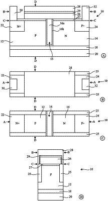
1. A memory cell comprising:
a first doped well of a first conductivity type in contact with a second doped well of a second conductivity type, the second conductivity type being opposite to the first conductivity type;
a third doped well of the second conductivity type in contact with a fourth doped well of the first conductivity type;
a first wall in contact with the second and fourth doped wells, the first wall comprising a conductive or semiconductor core and an insulating sheath;
a stack of layers comprising a first insulating layer, a first semiconductor layer, a second insulating layer and a second semiconductor layer at least partially covering the second and fourth doped wells; and
a third semiconductor layer located below the second and fourth doped wells and the first wall.
|