| CPC H10B 41/20 (2023.02) [H10B 41/41 (2023.02); H10B 43/20 (2023.02); H10B 43/40 (2023.02); H10B 41/10 (2023.02); H10B 43/10 (2023.02)] | 20 Claims |

|
1. A three-dimensional memory device, comprising:
a first alternating stack of first insulating layers and first electrically conductive layers;
an inter-tier dielectric layer located over the first alternating stack;
a second alternating stack of second insulating layers and second electrically conductive layers located over the inter-tier dielectric layer;
a memory opening vertically extending through the second alternating stack, the inter-tier dielectric layer, and the first alternating stack; and
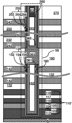
a memory opening fill structure located in the memory opening and comprising a first vertical semiconductor channel vertically extending through the first alternating stack and having a doping of a first conductivity type, a second vertical semiconductor channel vertically extending through the second alternating stack and having a doping of the first conductivity type, and an inter-tier doped region having a doping of a second conductivity type located between the first and the second vertical semiconductor channels, and providing a first p-n junction with the first vertical semiconductor channel and providing a second p-n junction with the second vertical semiconductor channel.
|