| CPC H10B 12/30 (2023.02) [H01L 29/0649 (2013.01); H10B 12/482 (2023.02); H10B 12/488 (2023.02)] | 13 Claims |
|
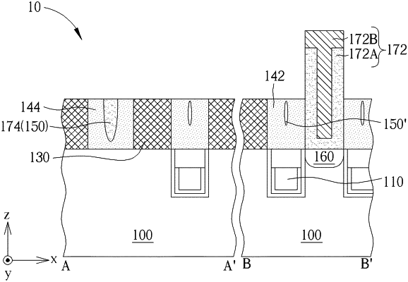
1. A semiconductor memory device, comprising:
a substrate;
a plurality of bit lines, disposed on the substrate and extending along a first direction;
a strip-shaped isolation structure, disposed at ends of the plurality of bit lines and extending along a second direction, wherein an upper portion of the strip-shaped isolation structure comprises a seam;
a conductive residue, disposed in the seam;
a plurality of columnar isolation structures, disposed between the bit lines and separated with each other; and
a plurality of conductive plugs, disposed between the bit lines and separated from each other, wherein the conductive residue and the conductive plugs comprise the same conductive material.
|