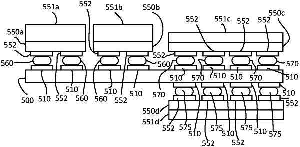
| CPC H05K 3/3494 (2013.01) [B23K 1/0016 (2013.01); B23K 35/262 (2013.01); H05K 3/3421 (2013.01); H05K 3/3489 (2013.01); B23K 2101/42 (2018.08)] | 23 Claims |

|
1. A method, comprising:
positioning a first solder between and in contact with one or more electrical contacts of a first electronic component and one or more mating first electrical contacts of a printed circuit board (PCB);
then heating the first solder to a first temperature to reflow the first solder;
then allowing the reflowed first solder to cool to form one or more first solder joints attaching the electrical contacts of the first electronic component to the first electrical contacts of the PCB;
then positioning a second solder in contact with one or more electrical contacts of a second electronic component and one or more mating second electrical contacts of the PCB;
then heating the second solder to a second temperature that is lower than the first temperature to reflow the second solder without reflowing the first solder joints;
then allowing the reflowed second solder to cool to form one or more second solder joints attaching the electrical contacts of the second electronic component to the second electrical contacts of the PCB;
where the electrical contacts of the second electronic component comprise electrically conductive solder balls having a higher melting point temperature than the second solder; and where the method further comprises performing the following steps before positioning the second solder in contact with one or more electrical contacts of the second electronic component and one or more mating second electrical contacts of the PCB:
positioning the electrically conductive solder balls in contact with the electrical contacts of the second electronic component and heating the electrically conductive solder balls to a third temperature to reflow the solder balls, and
then allowing the reflowed solder balls to cool to attach the solder balls to the electrical contacts of the second electronic component,
where the second temperature is less than the melting point temperature of the solder of the solder balls;
where the positioning the second solder in contact with the one or more electrical contacts of the second electronic component and the one or more mating second electrical contacts of the PCB comprises positioning the second solder between the reflowed solder balls and the one or more mating second electrical contacts of the PCB;
where the heating the second solder to a second temperature that is lower than the first temperature comprises heating the second solder to the second temperature without reflowing the solder balls; and
where the allowing the reflowed second solder to cool to form the one or more second solder joints attaching the electrical contacts of the second electronic component to the second electrical contacts of the PCB comprises allowing the reflowed second solder to cool to form hybrid solder joints that attach the electrical contacts of the second electronic component to the mating second electrical contacts of the PCB.
|