| CPC H05K 3/06 (2013.01) [H05K 1/05 (2013.01); H05K 1/181 (2013.01); H05K 3/4644 (2013.01); H05K 2201/10113 (2013.01)] | 22 Claims |

|
1. A method for manufacturing a circuit board, the method comprising:
preparing a first substrate and a second substrate, wherein:
the first substrate comprises a convex post member formed at a top surface of the first substrate, and
the second substrate includes a first surface and a second surface opposite to the first surface, and comprises:
a first metal layer formed on at least the first surface, and
an opening through which a top surface of the post member is uncovered in a plan view;
bonding at least a portion of a top surface of the first substrate excluding the post member and the second surface of the second substrate so that the top surface of the post member is uncovered through the opening; and
forming a circuit pattern by removing a first portion of the first metal layer: wherein:
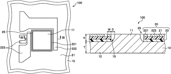
in the step of forming the circuit pattern, the first portion of the first metal layer is removed such that a second portion of the first metal layer continuously annularly surrounds a periphery of the post member in a plan view, and such that a width of the first metal layer surrounding the post member is in a range from 50 μm to 100 μm.
|