| CPC H05K 1/092 (2013.01) [C09D 11/037 (2013.01); H01B 1/026 (2013.01); H05K 3/1258 (2013.01); C09D 11/52 (2013.01)] | 19 Claims |

|
1. An electroconductive substrate comprising a base material and a metal wiring formed on at least one surface of the base material and made of at least either of silver and copper, wherein
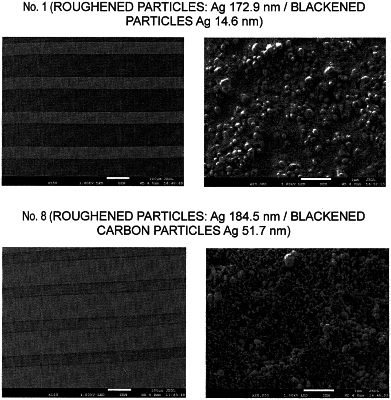
on part or all of a surface of the metal wiring, an antireflection region containing roughened particles that are made of at least either of silver and copper and blackened particles that are embedded between the roughened particles and finer than the roughened particles is formed,
the blackened particles are made of at least one of silver or a silver compound, copper or a copper compound, and carbon or an organic substance having a carbon content of 25 wt % or more, and
the antireflection region has a surface with a center line average roughness of 15 nm or more and 70 nm or less.
|