| CPC H05K 1/0298 (2013.01) [H05K 1/0313 (2013.01); H05K 1/05 (2013.01); H05K 1/09 (2013.01); H05K 1/11 (2013.01)] | 29 Claims |

|
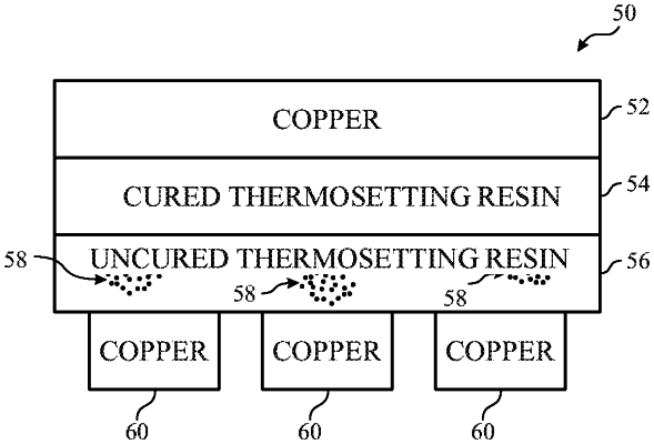
1. A multi-layered board, comprising:
a copper substrate; and
a bilayer dielectric, wherein the bilayer dielectric comprises:
a C-stage epoxy layer, wherein the C-stage epoxy layer is fully cross-linked and coupled to the copper substrate, wherein the C-stage epoxy layer comprises an amount of contamination of 1000 conductive materials per cubic meter or less; and
a B-stage epoxy layer, wherein the B-stage epoxy layer is partially cross-linked, wherein the B-stage epoxy layer is configured to transform into the C-stage epoxy layer via lamination of the B-stage epoxy layer and one or more copper traces, wherein the lamination comprises the B-stage epoxy layer being coupled to the one or more copper traces, and wherein the C-stage epoxy layer has a lower amount of contamination than the B-stage epoxy layer.
|