| CPC H05F 3/04 (2013.01) [H01H 9/48 (2013.01); H01H 13/70 (2013.01); H05K 5/0017 (2013.01)] | 17 Claims |

|
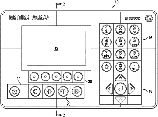
1. An assembly for protecting, from electrostatic discharge, a plastic keypad having data entry elements and at least one display element, the assembly comprising:
an overlay substrate, having a top side and a back side, the overlay substrate further having a plurality of precisely-positioned vias formed therethrough, the top side having a top surface coated with a static-dissipative layer of a conductive polymer and the back side having a back surface printed with at least one layer of color ink, the at least one layer of color ink depicting a plurality of alpha-numerical and pictorial elements of the keypad; and
an electrically-conductive arrangement, disposed on the overlay substrate to collect electrostatic charges on the top side, transfer the electrostatic charges to the back side through the plurality of vias and drain the transferred electrostatic charges to a ground, said electrically-conductive arrangement comprising:
at least one first conductive grid printed onto the top surface of the overlay substrate beneath the layer of conductive polymer, the at least one first conductive grid dividing the top surface into a plurality of surrounded areas, each of which is equal to or smaller than a predetermined size, each of the first conductive grids comprising a plurality of nodes, each node positioned atop, and extending into, a corresponding one of the plurality of precisely-placed vias;
at least one second conductive grid printed onto the back surface of the overlay substrate, below the at least one layer of color ink, such that each second conductive grid corresponds in size and shape to one of the first conductive grids, each of the second conductive grids comprising a plurality of nodes, each node positioned below, and extending into, a corresponding one of the plurality of precisely-placed vias; and
at least one conductive connection that communicates to ground each second conductive grid.
|