| CPC H04N 25/79 (2023.01) [H04N 25/131 (2023.01); H04N 25/134 (2023.01); H04N 25/65 (2023.01); H04N 25/766 (2023.01); H04N 25/77 (2023.01); H04N 25/78 (2023.01)] | 16 Claims |

|
1. A solid-state imaging device comprising:
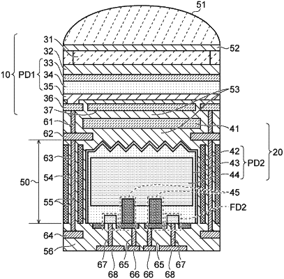
a first sensor that detects light in a first wavelength band;
a second sensor that detects light of a second wavelength band different from the first wavelength band, wherein
the first sensor includes a first pixel that detects light of the first wavelength band in incident light, and
the second sensor includes a second pixel that detects light in the second wavelength band that has transmitted through the first pixel among the incident light,
the first pixel includes a first photoelectric conversion section that photoelectrically converts the light of the first wavelength band,
the second pixel includes a second photoelectric conversion section that photoelectrically converts the light of the second wavelength band, and
the second photoelectric conversion section is disposed on a surface side of the first photoelectric conversion section opposite to a light incident surface of the first wavelength band;
a first chip including the first pixel and the second pixel; and
a second chip including a driving unit that drives the first pixel and the second pixel, and a readout section that reads out a pixel signal from the first pixel and the second pixel, wherein
the first chip and the second chip are stacked chips configured by being bonded to each other, and wherein
the driving unit includes
a first driving unit that supplies a control signal to the first pixel, and
a second driving unit that supplies a control signal to the second pixel, and
the readout section includes
a first readout section that reads out the first pixel signal generated by the first pixel, and
a second readout section that reads out the second pixel signal generated by the second pixel.
|