| CPC H04N 25/75 (2023.01) [H01L 27/14612 (2013.01); H01L 27/14636 (2013.01); H04N 25/79 (2023.01)] | 10 Claims |

|
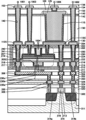
1. An imaging device comprising a first layer, a second layer, and a third layer,
wherein the second layer is provided between the first layer and the third layer,
wherein the first layer comprises a photoelectric conversion device,
wherein the second layer comprises a first circuit and a second circuit,
wherein the third layer comprises a third circuit and a fourth circuit,
wherein the first circuit and the photoelectric conversion device are configured to generate imaging data,
wherein the third circuit is configured to read the imaging data,
wherein the second circuit is configured to store the imaging data read by the third circuit,
wherein the fourth circuit is configured to read the imaging data stored in the second circuit,
wherein the second circuit comprises a first transistor and a first capacitor,
wherein one of a source and a drain of the first transistor is electrically connected to one electrode of the first capacitor,
wherein the other of the source and the drain of the first transistor is electrically connected to the third circuit,
wherein the other of the source and the drain of the first transistor is electrically connected to the fourth circuit, and
wherein the first transistor comprises a metal oxide in a channel formation region.
|