| CPC H04N 25/63 (2023.01) [H01L 27/14621 (2013.01); H01L 27/14627 (2013.01); H04N 23/54 (2023.01); H04N 23/55 (2023.01); H04N 25/61 (2023.01)] | 17 Claims |
|
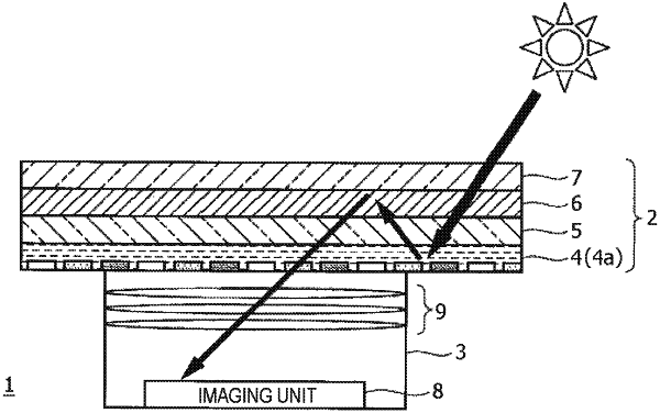
1. Electronic equipment comprising:
a display;
an imager that is disposed on a side opposite to a display surface of the display; and
a signal processor, wherein
the imager includes a plurality of on-chip lenses and a plurality of pixels,
the on-chip lens includes a first on-chip lens,
the plurality of pixels includes a first pixel, the first pixel being disposed to overlap the first on-chip lens,
the first pixel includes a plurality of photoelectric conversion units,
the signal processor processes signals output from the plurality of pixels, and
the signal processor corrects an output value of the first pixel in a case where output values from the photoelectric conversion units of the first pixel exceed a predetermined difference or a predetermined ratio.
|