| CPC H04N 23/843 (2023.01) [H04N 25/11 (2023.01)] | 20 Claims |

|
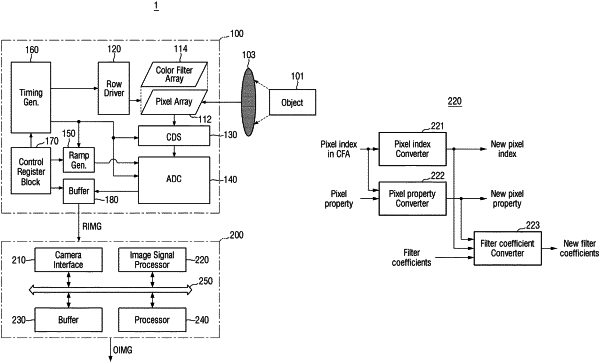
1. An image processing device comprising:
an image sensor having a plurality of unit groups, each unit group comprising a reference group and a conversion group each including a plurality of pixels and a plurality of color filters, the image sensor configured to generate image data using the plurality of pixels; and
an image signal processor configured to calculate a hash of the image data, and to select a filter corresponding to the hash to perform filtering,
wherein the image signal processor includes:
a pixel index converter configured to convert indexes of the plurality of pixels based on a positional relationship between the plurality of pixels,
a pixel property converter configured to convert the hash and properties of the plurality of pixels, and
a filter coefficient converter configured to convert filter coefficients of the plurality of pixels based on the respective converted pixel index and the respective converted pixel property,
wherein the conversion group includes a plurality of conversion regions, and the pixel index converter is configured to convert a pixel index of each of the plurality of conversion regions into a pixel index of the reference group based on a respective positional relationship.
|