US 12,034,585 B2
Modulation scheme conversion device and gateway
Jin Hwan Jung, Daejeon (KR); Song Min Kim, Daejeon (KR); Ji Hoon Ryoo, Incheon (KR); and Yung Yi, Daejeon (KR)
Assigned to KOREA ADVANCED INSTITUTE OF SCIENCE AND TECHNOLOGY, Daejeon (KR)
Appl. No. 17/763,496
Filed by KOREA ADVANCED INSTITUTE OF SCIENCE AND TECHNOLOGY, Daejeon (KR)
PCT Filed Aug. 3, 2020, PCT No. PCT/KR2020/010238
§ 371(c)(1), (2) Date Sep. 22, 2022,
PCT Pub. No. WO2021/060694, PCT Pub. Date Apr. 1, 2021.
Claims priority of application No. 10-2019-0117742 (KR), filed on Sep. 24, 2019.
Prior Publication US 2023/0013763 A1, Jan. 19, 2023
Int. Cl. H04L 27/36 (2006.01); G06K 19/07 (2006.01)
CPC H04L 27/36 (2013.01) [G06K 19/07 (2013.01)] 18 Claims
OG exemplary drawing
 
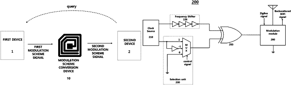
1. A modulation scheme conversion device comprising:
a backscattering tag to which a tag signal is provided; and
a tag signal generation unit configured to generate the tag signal,
wherein the modulation scheme conversion device multiplies a radio signal, which has been modulated with a first modulation scheme, and the tag signal to produce a multiplied signal and to reshape the multiplied signal with a second modulation scheme to produce a reshaped signal and backscatters the reshaped signal,
wherein the reshaping is performed in a physical (PHY) layer.