| CPC H03K 19/1776 (2013.01) [H03K 19/17744 (2013.01)] | 20 Claims |
|
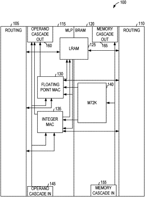
1. A circuit comprising:
a first memory circuit operable to:
receive an address input from a connection fabric of a field programmable gate array (FPGA), an intra-tile connection, or a cascade connection; and
provide a first data output based on the address input;
a second memory circuit operable to:
receive the address input; and
provide a second data output based on the address input; and
a multiplexer operable to:
receive a configuration input; and
based on the configuration input, provide either the first data output or the second data output.
|