| CPC H03K 19/017509 (2013.01) [H03F 3/45475 (2013.01)] | 20 Claims |
|
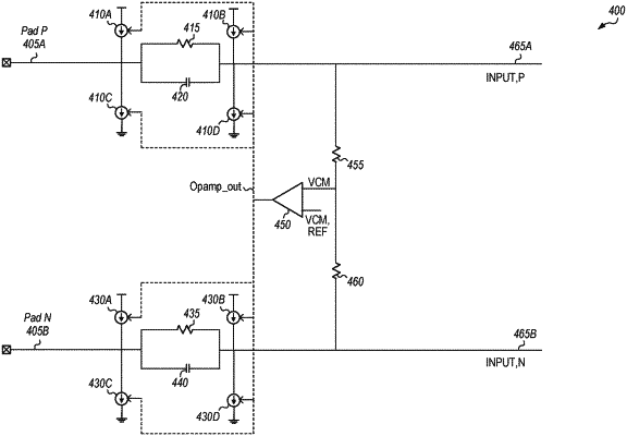
1. An apparatus comprising:
a first interface configured to receive a first input signal from a transmission line;
a circuit coupled to the first interface and configured to generate an output signal as a baseline wander corrected version of the first input signal, wherein the circuit comprises:
a resistor-capacitor parallel arrangement; and
one or more current sources connected to a first end of the resistor-capacitor parallel arrangement; and
one or more current sources connected to a second end of the resistor-capacitor parallel arrangement, wherein each current source on each of the first end and the second end is configured to receive a control signal based on a sensed common mode voltage of the first input signal and a second input signal different from the first input signal; and
a second interface configured to receive the output signal from the circuit.
|