| CPC H03F 3/72 (2013.01) [H01Q 1/526 (2013.01); H03F 1/56 (2013.01); H03F 3/19 (2013.01); H03F 3/211 (2013.01); H03H 2/008 (2013.01)] | 17 Claims |

|
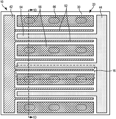
1. A radio frequency (“RF”) transistor amplifier, comprising:
an RF transistor amplifier die having a Group III nitride-based semiconductor layer structure and gate fingers, drain fingers and source fingers extending on an upper surface of the semiconductor layer structure; and
a plurality of conductive pillars extending perpendicular to the upper surface of the semiconductor layer structure, the conductive pillars including a first conductive pillar that is electrically connected to either the gate fingers or the drain fingers and first and second conductive ground pillars that are on opposed sides of the first conductive pillar, the first and second conductive ground pillars electrically connected to the source fingers,
wherein the first conductive pillar vertically overlaps an active region of the RF transistor amplifier die.
|