| CPC H03F 3/195 (2013.01) [H03F 1/0211 (2013.01); H03F 3/68 (2013.01); H03F 3/72 (2013.01); H04B 1/0458 (2013.01); H04B 1/0483 (2013.01); H04B 1/44 (2013.01); H03F 2200/294 (2013.01); H03F 2200/372 (2013.01); H03F 2200/451 (2013.01); H03F 2200/489 (2013.01); H04B 2001/0416 (2013.01)] | 4 Claims |

|
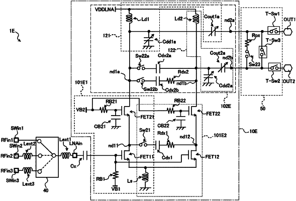
1. A semiconductor circuit comprising:
an input terminal to which a signal is supplied;
an input matching circuit connected to the input terminal;
a first circuit including a first transistor and a second transistor which are arranged in cascode connection;
a second circuit including a third transistor and a fourth transistor which are arranged in cascode connection;
a first output matching circuit connected to the first circuit;
a second output matching circuit connected to the second circuit;
a first passive circuit connected to a drain of the first transistor and a drain of the third transistor, and comprising at least one first passive element;
a second passive circuit connected to a drain of the second transistor and a drain of the fourth transistor, and comprising at least one second passive element;
a third passive circuit connected between a first output node of the first output matching circuit and a second output node of the second output matching circuit, and including at least one third passive element;
a first switch circuit connected between a first output terminal and the first output matching circuit;
a second switch circuit connected between a second output terminal and the second output matching circuit; and
a third switch circuit connected between the first output node of the first output matching circuit and the second output node of the second output matching circuit,
wherein
a source of the first transistor and a source of the third transistor are connected to an inductor,
a gate of the first transistor and a gate of the third transistor are connected to a first node to which the signal is supplied from the input terminal,
the first node is connected to the input terminal via the input matching circuit,
a source of the second transistor is connected to the drain of the first transistor,
a source of the fourth transistor is connected to the drain of the third transistor,
the drain of the second transistor is connected to a second node,
the drain of the fourth transistor is connected to a third node,
a gate of the second transistor and a gate of the fourth transistor are connected to a voltage terminal,
the first output matching circuit is connected between the second node and the fourth node,
the second output matching circuit is connected between the third node and the fifth node,
the fourth node is connected to the fifth node via the third passive circuit,
the first switch circuit is connected between the fourth node and the first output terminal,
the second switch circuit is connected between the fifth node and the second output terminal, and
the third switch circuit is connected between the fourth node and the fifth node.
|