| CPC H03F 1/42 (2013.01) [H03F 3/04 (2013.01); H03M 1/12 (2013.01); H03F 3/30 (2013.01); H03F 3/45 (2013.01); H03F 2200/36 (2013.01)] | 20 Claims |

|
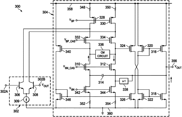
16. An analog-to-digital conversion circuit, comprising:
an analog-to-digital converter; and
a voltage reference coupled to the analog-to-digital converter, the voltage reference including:
a reference voltage circuit; and
an amplifier coupled between the reference voltage circuit and the analog-to-digital converter, the amplifier including:
a first stage including differential outputs and differential inputs, a first of the differential inputs coupled to the reference voltage circuit; and
a second stage including:
a single-ended output coupled to a second of the differential inputs;
a first output transistor configured to source current to the single-ended output;
a second output transistor configured to sink current from the single-ended output;
a third transistor coupled to a first of the differential outputs, and configured to drive the first output transistor;
a fourth transistor coupled to a second of the differential outputs, and configured to drive the second output transistor; and
a compensation network coupled to the single-ended output, the third transistor, and the fourth transistor, and configured to:
compensate the third transistor and the fourth transistor based on a signal at the single-ended output.
|