| CPC H03B 15/003 (2013.01) [G06N 10/20 (2022.01); G06N 10/40 (2022.01); H01P 7/08 (2013.01); H01P 7/105 (2013.01); H03H 7/01 (2013.01); H10N 60/12 (2023.02); G06N 10/00 (2019.01); H03B 2201/02 (2013.01)] | 11 Claims |
|
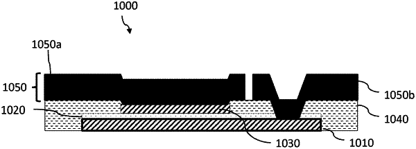
1. A method of fabricating a superconducting parallel plate capacitor, the method comprising:
depositing a first superconductive layer, the first superconductive layer comprising a material that is superconductive in a range of critical temperatures;
depositing a first dielectric layer to overlie at least part of the first superconductive layer;
depositing a second superconductive layer to overlie at least part of the dielectric layer, the second superconductive layer comprising a material that is superconductive in the range of critical temperatures;
removing a portion of the second superconductive layer to form at least one structure from the second superconductive layer and to expose at least part of the first dielectric layer;
depositing a second dielectric layer to overlie at least part of the second superconductive layer and at least part of the first dielectric layer;
planarizing the second dielectric layer;
removing at least part of the second dielectric layer to form a first via exposing at least part of the second superconductive layer;
removing at least part of the second dielectric layer and at least part of the first dielectric layer to form a second via exposing at least part of the first superconductive layer;
depositing a first region of a third superconductive layer; and
depositing a second region of the third superconductive layer, wherein the first region of the third superconductive layer is electrically isolated from the second region of the third superconductive layer, the first region of the third superconductive layer is superconductingly connected to at least part of the second superconductive layer by way of the first via, and the second region of the third superconductive layer is superconductingly connected to at least part of the first superconductive layer by way of the second via.
|