| CPC H02J 7/0069 (2020.01) [H01G 11/06 (2013.01); H01G 11/10 (2013.01); H01M 4/5825 (2013.01); H01M 10/0525 (2013.01); H01M 10/441 (2013.01); H02J 7/0024 (2013.01); H01M 10/4207 (2013.01)] | 10 Claims |

|
1. A power storage system comprising:
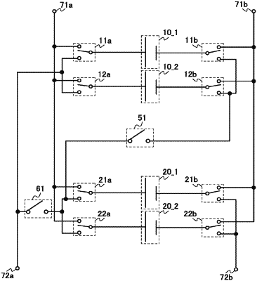
a first power storage element;
a second power storage element;
a third power storage element;
a fourth power storage element;
a first switch;
a second switch;
a third switch;
a fourth switch;
a fifth switch;
a sixth switch;
a seventh switch;
a eighth switch;
a ninth switch; and
a tenth switch,
wherein each of the first to eighth switches comprises a first transistor and a second transistor,
wherein one of a source and a drain of the first transistor is electrically connected to one of a source and a drain of the second transistor in each of the first to eighth switches,
wherein the one of the source and the drain of the first transistor in the first switch is electrically connected to a positive electrode of the first power storage element,
wherein the one of the source and the drain of the first transistor in the second switch is electrically connected to a negative electrode of the first power storage element,
wherein the one of the source and the drain of the first transistor in the third switch is electrically connected to a positive electrode of the second power storage element,
wherein the one of the source and the drain of the first transistor in the fourth switch is electrically connected to a negative electrode of the second power storage element,
wherein the one of the source and the drain of the first transistor in the fifth switch is electrically connected to a positive electrode of the third power storage element,
wherein the one of the source and the drain of the first transistor in the sixth switch is electrically connected to a negative electrode of the third power storage element,
wherein the one of the source and the drain of the first transistor in the seventh switch is electrically connected to a positive electrode of the fourth power storage element,
wherein the one of the source and the drain of the first transistor in the eighth switch is electrically connected to a negative electrode of the fourth power storage element,
wherein the other of the source and the drain of the first transistor in each of the first switch, the third switch, the fifth switch, and the seventh switch is electrically connected to a first connection terminal,
wherein the other of the source and the drain of the first transistor in each of the second switch, the fourth switch, the sixth switch, and the eighth switch is electrically connected to a second connection terminal,
wherein the other of the source and the drain of the second transistor in each of the first switch and the third switch is electrically connected to a third connection terminal and a first terminal of the tenth switch,
wherein the other of the source and the drain of the second transistor in each of the second switch and the fourth switch is electrically connected to a first terminal of the ninth switch,
wherein the other of the source and the drain of the second transistor in each of the fifth switch and the seventh switch is electrically connected to a second terminal of the ninth switch and a second terminal of the tenth switch,
wherein the other of the source and the drain of the second transistor in each of the sixth switch and the eighth switch is electrically connected to a fourth connection terminal,
wherein the first to tenth switches are controlled so as to switch between serial connection and parallel connection of the first to fourth power storage elements,
wherein the first to fourth power storage elements are charged by the parallel connection, and
wherein the first to fourth power storage elements are discharged by the serial connection.
|