| CPC H01S 5/18327 (2013.01) [H01S 5/0207 (2013.01); H01S 5/18341 (2013.01); H01S 5/18369 (2013.01); H01S 5/2022 (2013.01); H01S 5/2219 (2013.01); H01S 5/34333 (2013.01); H01S 5/04253 (2019.08); H01S 5/04256 (2019.08); H01S 2301/176 (2013.01); H01S 2304/12 (2013.01)] | 14 Claims |

|
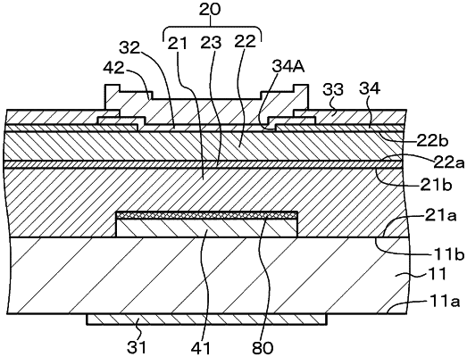
1. A light emitting element including a first light reflecting layer, a laminated structure, and a second light reflecting layer laminated to each other, wherein
the laminated structure includes a first compound semiconductor layer, a light emitting layer, and a second compound semiconductor layer laminated to each other from a side of the first light reflecting layer,
light from the laminated structure is emitted to an outside via the first light reflecting layer or the second light reflecting layer,
the first light reflecting layer has a structure in which at least two types of thin films are alternately laminated to each other in plural numbers,
a film thickness modulating layer is provided between the laminated structure and the first light reflecting layer,
at least two light absorbing material layers are formed inside the laminated structure in parallel with a virtual plane occupied by the light emitting layer, and
0.9×{(m·λ0)/(2·neq)}≤LAbs≤1.1×{(m·λ0)/(2·neq)}
is satisfied when an oscillating wavelength is λ0, an entire equivalent refractive index of two light absorbing material layers and a portion of the laminated structure positioned between the two light absorbing material layers is neq, and a distance between the two light absorbing material layers is LAbs, and m is one.
|