| CPC H01Q 5/371 (2015.01) [H01Q 1/38 (2013.01)] | 20 Claims |

|
1. An electronic device comprising:
a housing;
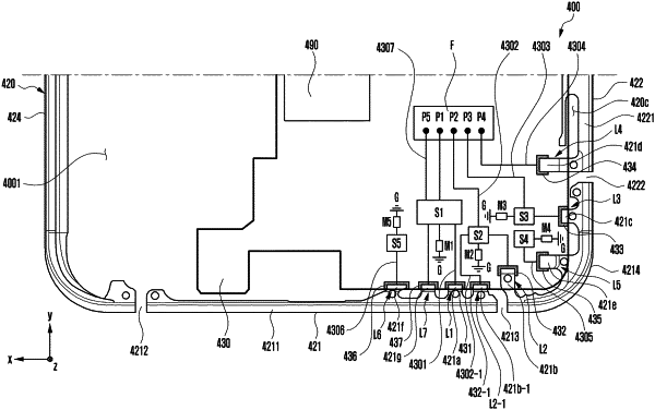
a side member disposed in at least some of the housing and including a first side surface, a second side surface extending perpendicular to one end of the first side surface, a third side surface extending parallel to the first side surface from the second side surface, a fourth side surface connected from the third side surface to the first side surface and parallel to the second side surface, a first conductive portion disposed between a first non-conductive portion and a second non-conductive portion spaced apart at a specified interval in the first side surface, and a second conductive portion disposed between the second non-conductive portion and a third non-conductive portion formed on the second side surface;
a substrate disposed in an internal space of the housing and including a ground;
at least one wireless communication circuit disposed on the substrate;
a first switching circuit disposed in a first electrical path connecting the at least one wireless communication circuit and a first point of the first conductive portion;
a second switching circuit disposed in a second electrical path connecting the at least one wireless communication circuit and a second point of the second conductive portion;
a third switching circuit disposed in a third electrical path connecting the at least one wireless communication circuit and a third point of the second conductive portion between the second point and the third non-conductive portion; and
at least one processor configured to control at least one switching circuit among the first, second, and third switching circuits,
wherein the second switching circuit is electrically connected to another—first point between the first point and the second non-conductive portion through another—first electrical path.
|