| CPC H01Q 17/00 (2013.01) [H01Q 1/38 (2013.01); H01Q 1/42 (2013.01); G01S 13/931 (2013.01)] | 10 Claims |
|
1. A radar sensor, comprising:
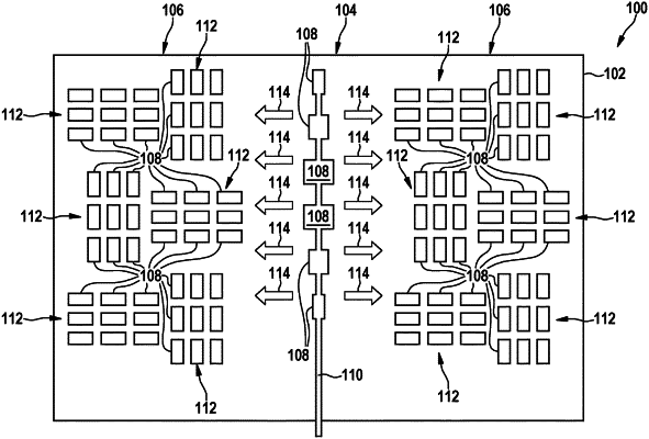
an antenna structure formed of (a) a plurality of emitters having respective emission surfaces and (b) an electrically conductive line physically connecting the plurality of emitters to one another and to control electronics, the control electronics being configured to generate an electrical signal provided to the plurality of emitters via the electrically conductive line causing the plurality of emitters to emit radar waves in a first direction towards an exterior of the radar sensor;
a coupling structure formed of at least one emitter that each has a respective emission surface that faces in the first direction and is electrically insulated from all other components of the radar sensor, so that the at least one emitter is electrically insulated from (a) the antenna structure, (b) the electrically conductive line, and (c) the control electronics;
a substrate carrying the antenna structure and the coupling structure; and
an absorber having an absorption surface facing opposite the first direction, towards the emission surface of the at least one emitter, wherein:
the coupling structure is configured to emit, via the emission surface of the at least one emitter of the coupling structure, substrate waves from the substrate as coupled waves in the first direction towards the absorption surface of the absorber; and
the absorber is configured to absorb the coupled waves emitted by the coupling structure.
|