| CPC H01L 33/62 (2013.01) [H01L 27/156 (2013.01); H01L 33/005 (2013.01); H01L 33/38 (2013.01); H01L 2933/0016 (2013.01); H01L 2933/0066 (2013.01)] | 20 Claims |

|
1. An assembly board for use in a display manufacturing method for allowing semiconductor light emitting diodes to be seated at preset positions on the assembly board using an electric field and a magnetic field, the assembly board comprising:
a base portion;
a plurality of assembly electrodes extending in one direction and disposed on the base portion at predetermined intervals;
a dielectric layer stacked on the base portion to cover the plurality of assembly electrodes;
barrier ribs stacked on the dielectric layer and defining cells in which semiconductor light emitting diodes are seated at the predetermined intervals along an extending direction of the plurality of assembly electrodes so as to overlap a portion of the plurality of assembly electrodes; and
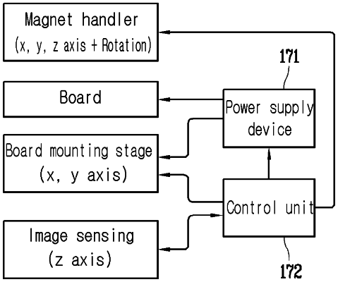
a voltage applying unit connected to at least opposite ends of the plurality of assembly electrodes to apply one or more voltage signals to the plurality of assembly electrodes,
wherein a voltage signal of the same polarity is applied to the plurality of assembly electrodes from the voltage applying unit connected to the opposite ends.
|