| CPC H01L 33/62 (2013.01) [G09G 3/32 (2013.01); H01L 25/0753 (2013.01); G09G 2300/0426 (2013.01); H01L 25/167 (2013.01)] | 14 Claims |

|
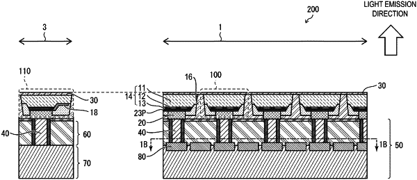
1. An image display element comprising:
a plurality of micro light-emitting elements arrayed in an array manner; and
a semiconductor layer at which a drive circuit is disposed, the drive circuit being configured to supply a current to each of the plurality of micro light-emitting elements to emit light, wherein
the drive circuit comprises a transistor, the transistor and a wiring layer are disposed at a first surface of the semiconductor layer,
the plurality of micro light-emitting elements is disposed at a second surface of the semiconductor layer that is an opposite side of the first surface,
the transistor and the wiring layer are electrically coupled to the plurality of micro light-emitting elements through a through substrate via that extends through the semiconductor layer,
the plurality of micro light-emitting elements includes:
a first electrode disposed at a light emitting surface side of the plurality of micro light-emitting elements; and
a second electrode having a polarity opposite a polarity of the first electrode and disposed at a surface at an opposite side of the light emitting surface, and
the second electrode is electrically conductive to the through substrate via.
|